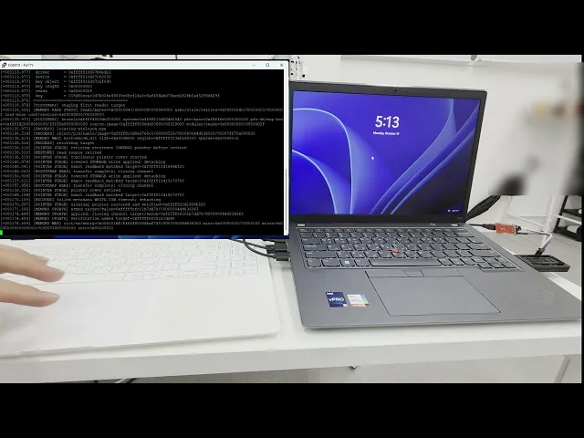


Demo
The attack itself requires only the USB device. The UART connection is used solely to show progress during the demo.
1. Introduction
The video above shows what happens when we plug our custom USB device into a locked Windows 11 machine in its default state.
Demo conditions:
Clean Windows 11 25H2 (build 26200.9278)
VBS and HVCI enabled
Locked screen
No network connection required
No third-party drivers required
No local helper process required
No user interaction required
Single USB insertion
Under these conditions, our FPGA USB device obtains arbitrary kernel read/write, extracts the BitLocker full volume encryption key (FVEK), and then patches the logon process to bypass the screen lock. All the attack logic runs on the USB device. The extracted FVEK allowed us to mount the BitLocker-protected volume with Dislocker and recover files, while the logon patch allowed us to unlock the Windows session by entering any password.
There is a large gap between a single crash log and a working attack chain. Bridging it meant chaining primitives, working around mitigations, and agonizing over why an exploit silently failed. This weaponization phase took far more effort than finding the bug, and it is where most of our time went.
There are no Hollywood tricks here. The device is custom hardware and firmware built from scratch, and this three-part series breaks down how it works.
Series structure and release timing
This work is an internal research project conducted by the System Security Research Lab at ENKI WhiteHat starting in early 2026. We plan to release the results in three parts.
Part 1 (this post), hardware: why off-the-shelf tools were insufficient, how we built the USB controller and board ourselves, what is on the board, and how we debugged a device designed from scratch.
Part 2, vulnerability and exploit: which code is vulnerable and why, and the process of building a repeatable kernel read from a limited primitive.
Part 3, post-exploit: what becomes possible once kernel read and write are obtained.
Parts 2 and 3 are currently on hold pending coordinated disclosure. During the broader research effort, we also reported vulnerabilities beyond the ones discussed in this series; CVE assignment is still pending for most of them. Some bugs in our chain were patched in September 2026 after another researcher reported them. We had found them independently but had not reported them at that time, since we were still assessing their exploitability and chaining them with other vulnerabilities. The remaining reports are still going through coordinated disclosure.
Part 2 will carry the technical detail once that process finishes. We plan to release Part 2 and Part 3 later, as a conference talk or as blog posts.
The hardware in Part 1 is not tied to any specific vulnerability, so we are releasing it first.
2. Why we needed an FPGA
At the hardware level, our goal came down to a single requirement:
Make a single USB connection appear to the host as many independent USB devices at the same time.
The host needed to see a hub and a large number of downstream devices, each with its own USB address and endpoint state, over one physical USB link. We needed those devices to remain connected simultaneously so Windows would keep their kernel objects allocated while it created objects for other devices. This let us shape the kernel pool through USB traffic alone.
When a USB device is attached, the host enumerates it by querying its device, configuration, string, and class descriptors. Because the device controls every byte in those responses, and Windows parses them even while the screen is locked, enumeration gives an external device a direct path into the kernel's USB stack. While our target vulnerability in the Windows kernel (covered in Part 2) does not depend on tight USB timing to trigger, turning that bug into a reliable exploit imposes strict requirements on the hardware.
Another bug we investigated was a timing-sensitive use-after-free caused by a race condition. To trigger it reliably, we needed to control the timing of USB transactions and widen the window in which the freed object could be accessed before it was reused. NAK backpressure gave us that control by letting the device delay a transaction. Commodity USB cores and MCUs generally do not expose this kind of control, since ordinary devices have no reason to deliberately stall transactions. With the FPGA, we could implement the delay in RTL, which substantially improved the reproduction rate, but not enough to keep the bug in the exploit chain.
Pool grooming over USB
Triggering a memory corruption bug is very different from weaponizing it. Most memory bugs offer only a narrow primitive: writing a few bytes past an object boundary, reading slightly out of bounds, or returning uninitialized memory. On its own, triggering such a bug usually causes a crash, does nothing, or leaks useless bytes. Turning that bug into a working exploit requires placing useful target data, like kernel pointers or length fields, directly adjacent to the vulnerable buffer. Placing the kernel pool into that state requires pool grooming (or heap spraying): issuing a controlled sequence of allocations and frees to shape the memory layout before triggering the bug.
In a local privilege escalation exploit, pool grooming is straightforward: an unprivileged process can simply call native APIs in a loop to allocate thousands of event objects or pipes until the pool layout is ready, and then convert a narrow bug into a repeatable arbitrary address read/write (AAR/AAW) primitive.
In our USB-only exploit scenario, however, the screen is locked and we have no code execution on the target. All kernel allocations must be driven entirely from the USB bus. Fortunately, USB enumeration triggers a predictable set of kernel allocations: each newly attached device causes Windows to allocate a device object, configuration and interface structures, endpoint contexts, and class-driver state. Once enumeration completes, upper-layer drivers keep allocating. A mass storage device triggers volume mounting, metadata parsing, and file system cache allocations, while a HID device allocates and queues input reports. By controlling what descriptors and payloads the device returns, we can steer the size, count, and order of these kernel allocations just as a local exploit would with native APIs.
The catch is that we cannot keep the groomed pool layout intact by attaching and detaching devices one by one. When a USB device disconnects, Windows frees the kernel objects associated with it, tearing down the layout we just built. For earlier allocations to remain in place while new objects are slotted into adjacent holes, dozens of USB devices must stay alive on the bus simultaneously.
Typical microcontrollers with built-in USB device controllers do not support this directly. Their USB peripherals are designed around a single 7-bit device address register and a single set of endpoints tied to that address. While a composite device can expose multiple interfaces under one address, it still counts as a single device. Existing software-defined USB implementations on MCUs also generally assume a single device address, and they spend much of their CPU budget keeping up with bus synchronization. V-USB bit-bangs AVR GPIOs at low speed, and Pico-PIO-USB offloads full-speed bit timing to RP2040 PIO state machines.
To keep this many devices active at once, the controller must track per-address endpoint state in parallel, inspect the destination address of each incoming host token, and reply within the USB turnaround window, without knowing in advance which address the host will poll next. Meeting these scale and latency constraints meant moving to an FPGA, handling bit-level timing and parallel state lookups for numerous addresses in hardware.
Why existing USB setups were not enough
Most prior USB security research only needed a single device address at a time:
In our earlier Windows printer driver research (CVE-2026-32223 in
usbprint.sys), an Odroid C4 running Raw Gadget only had to present a single device descriptor while a local helper process on the target machine handled pool grooming and triggering.Plug and Pwn's physical zero-click chain used a FaceDancer setup to present Sierra and Sony device identities sequentially, with no user logged in on the target. Because only one identity was active at a time, a single device address was sufficient.
Address count is not the whole requirement. A controller must also sequence the attack: when each identity is attached, when it is detached, and what a device returns based on data an earlier device received. In “Gone in 60 Frames” (DEF CON 34), NCC Group's Exploit Development Group implemented that controller as a separate layer. Their D.U.E.T. framework coordinates multiple RP Pico boards over Wi-Fi, connecting and disconnecting devices on demand and transferring leaked data back to the attacker.
Connect and disconnect therefore had to be a firmware operation on a hub port rather than a physical event. Raw Gadget documents that it cannot emulate USB hubs. Cynthion's ECP5 FPGA can host custom gateware (multi-device emulation is tracked in issue #262), but it typically pairs its TARGET port with a host PC on the CONTROL port running Python attack scripts. An on-board controller also removes the companion machine, which the demo conditions require: no network, no helper process, a single insertion. That is why we designed both the USB controller and the PCB from scratch.
3. Building the board
First prototype on perfboard

Before laying out a custom PCB, we wired a USB connector to an Arrow MAX1000 development board on perfboard to verify that the FPGA I/O pins could drive and sample full-speed USB directly. We brought up a minimal system using a Nios V soft processor paired with an open-source USB device core that handled full-speed signaling and the Serial Interface Engine (SIE), leaving descriptor responses to the Nios V firmware.
To test the setup quickly, we plugged a standard desktop keyboard into the host through a Total Phase Beagle analyzer, recorded every enumeration transaction, and replayed those exact byte sequences from the firmware. The prototype enumerated as a keyboard on the first try, confirming that our perfboard wiring and direct FPGA I/O could reliably handle full-speed USB. It also hit the exact limitation we expected: the open-source USB core was hardcoded around a single device address and needed a ground-up rewrite to support dozens of concurrent devices.
Custom PCB


To turn the prototype into a self-contained dongle, we designed a custom PCB based on the published MAX1000 schematic (Arrow released only the schematic, so we routed the board layout from scratch). The largest change was the removal of the Arrow USB Blaster circuit. On the MAX1000, the USB port is a development interface wired to an FT2232H bridge that provides JTAG and UART; on our board, the USB port is the attack interface that plugs directly into the target PC. We replaced the receptacle with a male SMD USB-A plug, redesigned the power regulation stage, and substituted unavailable components. We also removed the LIS3DH 3-axis MEMS accelerometer, which our design does not use. JTAG and UART are broken out to headers along the edge; the board also carries status LEDs and two push buttons. During an actual attack, nothing needed to be attached to those headers. The board draws power directly from the target port and runs autonomously.
While waiting for PCB/A, we rewrote the gateware in parallel. We replaced the Nios V processor with the open-source NEORV32 core, ported the Migen/LiteX ValentyUSB eptri design to Verilog, and then redesigned the controller architecture around multi-address operation so the bitstream was ready to flash the day the boards arrived.
A self-contained multi-device controller
The photo below shows the multi-board USB setup presented by NCC Group as part of its D.U.E.T. framework. Multiple USB device boards connect through hubs; D.U.E.T. coordinates multiple RP Pico boards over Wi-Fi, enabling devices to be connected or disconnected on demand and data to be transferred between the devices and the attacker. Coordinating separate boards keeps each device independent and makes the setup easy to extend.

D.U.E.T. multi-board USB setup, shown in NCC Group's DEF CON 34 presentation.
Our design brings those roles onto one self-contained FPGA board. It presents the hub and numerous downstream USB addresses over one physical link, maintains per-address endpoint state in hardware, and responds to host tokens within the USB turnaround window. On-board NEORV32 firmware sequences the emulated devices and their behavior. Multi-device emulation, time-critical USB responses, and attack sequencing all happen on the device itself, so the attack needs no companion machine and no software on the target.
System architecture

At a high level, the board combines an FPGA-based SoC (housing our custom USB controller and a RISC-V core) with external SDRAM and SPI flash on a single PCB:
Component | Specification |
|---|---|
FPGA | Intel MAX 10 10M16SAU169C8G |
Clocks | 12 MHz input |
CPU | NEORV32, RV32IMC + Zba/Zbb/Zbs |
On-chip memory | 4 KiB boot ROM (IMEM), 8 KiB data RAM (DMEM) |
Cache | 4 KiB I-cache and 4 KiB D-cache, 64-byte line |
External memory | 32 MiB x16 SDR SDRAM (AS4C16M16SA), 8 MiB SPI flash for boot and data storage |
USB front end | No external PHY; FPGA I/O drives D+/D- and the pull-up directly |
Debug | UART, LED, push buttons |
An on-chip PLL derives two frequencies on three outputs from the 12 MHz board oscillator: a 48 MHz clock for the entire USB controller and a 72 MHz system clock for the CPU, SPI master, and SDRAM controller (with a phase-shifted copy of the 72 MHz clock routed to the SDRAM chip). Keeping the entire USB pipeline inside a single 48 MHz domain, with a clock-domain bridge for CPU MMIO accesses and a separate synchronizer for the USB IRQ, lets us close USB line timing independently of CPU memory and cache paths.
The system boots in two stages. A first-stage bootloader embedded in the 4 KiB on-chip IMEM reads a firmware container from the 8 MiB SPI flash, checks its keyed BLAKE2s-128 authentication tag, copies the main application into the 32 MiB external SDRAM, and jumps to it. Application code, static data, and the dynamic heap all reside in SDRAM, backed by 4 KiB instruction and data caches whose 64-byte cache lines match the SDRAM controller's burst length. The 8 KiB on-chip DMEM, which adds no external-bus wait states, holds the application stack.
This memory layout differs from embedded USB frameworks like Moondancer, where tight RAM budgets (tens of kilobytes) favor static buffers and zero dynamic allocation. Because our exploit state machine manages complex, variable-lifetime objects across dozens of emulated devices, we put the 32 MiB SDRAM to work as a general-purpose heap, while keeping deadline-critical USB endpoint state and packet buffers inside the FPGA's internal M9K block RAM.
4. Multi-address USB controller architecture
Splitting work between RTL and firmware
When designing the controller, we had to decide where to draw the line between Verilog RTL and C firmware. Putting descriptors, class protocols, and the exploit state machine into RTL would make iteration painfully slow; on the other hand, using the FPGA as a dumb PHY and handling every USB packet in software would miss USB turnaround deadlines.
On a full-speed bus, the host sends a token and expects a DATA packet or handshake (ACK, NAK, or STALL) within a few bit times. With a single device address, a fast interrupt handler might keep up, but when the host polls dozens of downstream addresses back to back, any interrupt latency or SDRAM cache miss will violate the turnaround window and register as a bus error.

To guarantee deterministic response times regardless of active device count, we split the workload strictly down the middle: firmware prepares the data, and hardware handles the wire.
The 48 MHz Verilog RTL owns everything on the token response deadline:
D+/D- pin sampling, drive enable, and 4x clock/data recovery (CDR)
NRZI encoding/decoding, bit stuffing, EOP/SE0 detection, and PID/CRC checks
Hardware lookup mapping a 7-bit USB bus address to an internal slot (0..63)
Per-slot, per-endpoint state (arm, stall, data toggle, and isochronous mode)
Immediate transaction responses (DATA0/DATA1, ACK, NAK, STALL) and automatic retries
Shared packet page allocation, completion queues, and per-slot event bitmaps
The 72 MHz NEORV32 C firmware owns higher-level protocol and attack logic:
Device, configuration, string, and class descriptors
Virtual hub port state machines (connect, disconnect, reset timing, and status change bits)
Class-level behavior
Pool grooming sequences, the exploit state machine, and UART logging
By design, the RTL knows nothing about Windows or the exploit. Firmware simply pre-loads the payload and arms the endpoint, leaving the hardware to complete the transaction on its own as soon as the host token arrives.
To keep the CPU from drowning in interrupts under full-speed polling, hardware events are exposed via two mechanisms over a 1 KiB MMIO region at 0xF0000000. Routine endpoint activity sets the slot's bit in a 64-bit event bitmap, and per-endpoint arm/have state is readable as a per-slot bitmap, so firmware can inspect endpoints at its own pace. OUT transactions push page descriptors into a hardware completion queue instead, because an incoming host packet must never be dropped or overwritten before software reads it. A Wishbone clock-domain bridge carries CPU register accesses between the 72 MHz and 48 MHz domains, while a separate three-flop synchronizer carries the level IRQ into the 72 MHz domain.
Soft PHY and the 48 MHz packet pipeline
Because the board has no external ULPI or UTMI transceiver chip, the FPGA's I/O buffers drive D+, D-, and the full-speed pull-up resistor directly.

On the receive path, each 12 Mbps full-speed bit spans four cycles of the 48 MHz clock. The clock-recovery block oversamples the differential line at 4x, realigns its phase on every line transition, and samples near the center of each bit cell:

Recovered bits pass through NRZI decoding and bit-stuff removal, shift into byte lanes, and are validated by the CRC checker before reaching the transaction engine. A packet-header decoder extracts the 7-bit address and 4-bit endpoint number from incoming tokens so the transaction engine can execute SETUP, OUT, or IN state machines. Those state machines enforce inter-packet turnaround times, DATA0/DATA1 toggle matching, retries, and isochronous rules without CPU intervention.
The transmit path runs this pipeline in reverse:
Outgoing payloads are framed with a PID and CRC16, bit-stuffed, NRZI-encoded, and registered directly onto the D+/D- output buffers so that internal pipeline depth never introduces jitter onto the wire.
64 addresses, 1,024 endpoints, and shared page pools
A USB token carries a 4-bit endpoint number (16 endpoint numbers per direction) and a 7-bit address field (allowing up to 127 addresses on a bus). Rather than supporting all 127 addresses, we sized our hardware tables for 64 concurrent device slots. That was enough for our pool-grooming sequence and allowed the per-slot bitmaps to fit cleanly into two 32-bit registers.
With 64 address slots and 16 endpoints per slot in both IN and OUT directions, the hardware tracks 1,024 logical endpoints per direction. When a token arrives on the wire, a hardware address table translates the 7-bit USB address into an internal slot index (0..63) before the rest of the token has even finished shifting in. Because 2,048 total endpoint contexts are far too large for flip-flop registers, endpoint state is packed into dual-port M9K block RAM, guarded by an arbiter and snapshot logic so firmware updates never collide with an in-flight USB transaction.
Still, dedicating a fixed 64-byte buffer to all 2,048 directional endpoints would demand 128 KiB of memory, nearly double the 68.6 KiB (562,176 bits) available on the MAX 10 10M16. To stay within the chip's BRAM budget, we decoupled endpoint state from payload storage.
Instead of per-endpoint buffers, payloads are allocated dynamically from a shared pool of sixty-four 64-byte pages (4 KiB) per direction. Even when dozens of devices are enumerated simultaneously, actual USB bus traffic is sparse: only a handful of endpoints hold live packets at any instant. An endpoint borrows a 64-byte page only while a transfer is active and returns it to the pool upon completion, with a small subset of pages reserved exclusively for EP0 control transfers so enumeration never deadlocks. If the shared pool ever fills up, bulk and interrupt endpoints automatically apply backpressure by replying NAK, while isochronous endpoints drop the packet and set an overflow flag for firmware to inspect.
Emulating a 63-port virtual hub

To expose up to 63 downstream devices through a single physical D+/D- pair, slot 0 operates as a 63-port full-speed virtual hub, while slots 1..63 represent the child devices attached to its ports.
Emulating this hub takes tight coordination between firmware and RTL. Firmware implements the USB hub class: it serves the hub descriptor, tracks per-port status and change bits across all 63 logical ports, runs timers for port-reset signaling, and responds to host requests for port power, reset, and suspend.
The RTL makes that topology behave like real hardware on the wire. When the host resets a hub port to enumerate a newly attached child device, firmware marks that port active and binds its corresponding slot (1..63) to USB default address 0. The hardware address table then routes any host tokens sent to address 0 directly to that child slot until SET_ADDRESS assigns it a permanent bus address. Meanwhile, every previously enumerated device on slots 1..63 continues responding to its own assigned address without interruption.
Synthesis and timing results
By subsystem, the custom USB core takes the largest share at 7,914 logic cells and 31 M9K blocks (mostly for the endpoint tables and page pools), followed by the NEORV32 CPU complex at 4,717 logic cells and 25 M9K blocks. The SDRAM controller (509 LCs, 1 M9K), SPI master (334 LCs), and Wishbone clock-domain bridge (167 LCs) make up the rest.
Total embedded memory bit utilization is only 58%, but 57 of 61 physical M9K blocks (93%) are in use, because narrow lookup tables, dual-port memories, and FIFOs of varying widths cannot pack every bit of a 9-kilobit block. Only four M9K blocks remain free on the entire FPGA, which is why separating endpoint state from shared payload pages was mandatory.
Under Quartus's Slow 1.2 V, 85 °C timing model, the 48 MHz USB domain achieves an Fmax of 51.87 MHz (1.555 ns setup slack) and the 72 MHz system domain reaches 78.38 MHz (1.130 ns setup slack), with a minimum hold slack of 0.204 ns across both domains.
5. Debugging across three layers
In standard exploit development, the underlying hardware and OS transport are known quantities. When an exploit fails, the bug is in your exploit code or your analysis of the target. Because we built both the USB controller and the board from scratch, every failure turned into a three-way guessing game: did the RTL violate the USB spec, did the C firmware mishandle state, or did the real machine do something unexpected?
Case study: A back-to-back MMIO request that vanished
One failure first appeared as a firmware trap rather than malformed USB traffic. The NEORV32 raised a store-access fault during an ordinary endpoint-control write. Mapping the faulting instruction against the exact firmware image showed that the access itself was valid, which pointed us toward the Wishbone clock-domain crossing between the 72 MHz CPU and the 48 MHz USB core.
The bridge handled one outstanding access at a time and assumed that CYC and STB would be deasserted after each ACK. NEORV32's XBUS can legally keep both signals asserted and present the next transfer immediately after the previous acknowledgement. The first access completed, but the bridge failed to recognize the second. The CPU then waited until the XBUS timeout expired and raised the store-access fault that we saw over UART.
We reproduced the sequence in a focused Verilog testbench using the production clock rates and two consecutive MMIO requests. With the original RTL, only the first request reached the USB domain. We changed the bridge to distinguish the next transfer from the one it had just acknowledged without requiring an idle cycle. The request capture is one condition:
The just-consumed ACK is what separates a new request from the one already in flight. Both requests then completed, while the existing cancellation behavior remained intact.
The UART fault log narrowed the problem to the clock-domain crossing, and the focused testbench reduced a minutes-long hardware cycle to a deterministic millisecond-scale regression.
The other two layers
Debugging the end-to-end attack chain against a locked Windows PC was harder. Beyond the RTL, failures could come from the C firmware or emerge only on the real target machine.
The C firmware had its own failure modes. One bug deadlocked the attack chain because a trigger was gated on a queue that the host would drain only after that trigger fired. Another allowed a bookkeeping store in interrupt context to overwrite a main-loop notification, leaving the host waiting for a message that had already been marked as sent. These were state-machine bugs rather than protocol issues. Their full stories belong in Part 2, alongside the exploit chain itself.
Windows supplied the third layer. Late in the chain, the target bugchecked with IRQL_NOT_LESS_OR_EQUAL at DISPATCH_LEVEL while reading an address our device had staged for the host. Every readback on our side said the data was in place. The same chain ran to completion in our QEMU-based development environment without crashing, so we needed the physical machine's crash dump to understand the failure. We return to this failure class in Part 2.
6. Demo walkthrough
With the hardware architecture in place, we can return to the demo. From the moment the board is plugged in, the entire sequence runs autonomously on the device.
Windows first sees a full-speed USB hub, followed by dozens of downstream devices. The firmware handles their enumeration while the RTL keeps each assigned address responsive on the same physical link. No companion computer or local helper process is involved.
As the sequence progresses, the USB device establishes kernel read and write access. There is no visible change on the Windows screen during this phase. The session remains locked while the firmware reports progress over UART.
At approximately 114 seconds after insertion, the device finishes locating and reading the BitLocker FVEK. The demo's UART output records the resolved object addresses and the key length. To validate the extracted FVEK, we used Dislocker to mount the BitLocker-protected volume. We successfully read and recovered files from the mounted volume, confirming that the extracted key gave us access to the encrypted data.
The device then modifies the logon process.
The visible result comes when an incorrect password is submitted: Windows accepts it and unlocks the existing desktop session.
Before finishing, the firmware restores the overwritten kernel pointers and staged structures used during the chain. The logon process stays patched, so the target keeps accepting any password at the lock screen.
Part 2 explains how the chain establishes kernel read and write access; Part 3 follows those primitives through key extraction and the lock-screen bypass.
7. Limitations and release plan
Hardware limitations
Looking back at the hardware design, our current board has three main constraints.
First, the soft PHY is limited to full-speed (12 Mbps) operation, which is the only constraint that narrows our research scope. Because the FPGA I/O pins drive the bus directly without an external transceiver, mass-storage emulation is limited to Bulk-Only Transport (BOT) over USBSTOR and cannot present UAS. A High-Speed or SuperSpeed PHY would open up UAS (and bulk streams).
Second, the 8 MiB SPI flash limits how much data the device can carry offline. The limit does not affect protocol capabilities or our current tests, only additional features or payloads we might bundle later.
Third, FPGA resource headroom is tight. As the synthesis results show, 86% of logic elements and 57 of 61 M9K blocks are already in use, with 1.130 ns of setup slack on the 72 MHz domain. Adding major new hardware features would exhaust M9K blocks first and make placement and timing closure harder after that. Moving to a larger FPGA is a decision we would make alongside upgrading the PHY.
Open-source release and stack
Once all vulnerabilities reported during this research have been patched, and after the necessary reviews, we plan to open-source the entire project, including the schematic, PCB layout, RTL, and exploit firmware.
Components used:
NEORV32: Stephan Nolting's VHDL RISC-V soft core, used unmodified behind a custom VHDL memory and peripheral wrapper
Custom USB core: our own Verilog implementation, redesigned from Sean Cross's ValentyUSB eptri, originally written in Migen/LiteX
Software and toolchain:
GCC: firmware compilation
Questa, Icarus Verilog: RTL simulation
Verilator, Verible: RTL linting
Quartus: synthesis and timing analysis
QEMU, rv32emu: the simulation environment used to develop the attack chain (covered in detail in Part 2 and Part 3)
Part 1 summary
With no local code execution on the target, the USB device has to drive kernel pool grooming entirely through enumeration and class traffic, keeping dozens of device addresses alive on the bus at once.
Off-the-shelf MCUs and software USB implementations are built around a single device address, whereas an FPGA can run bit-level timing and parallel per-address state management at the same time.
A 48 MHz soft PHY handles the full-speed wire protocol directly without an external transceiver, while hardware address and endpoint tables take firmware and SDRAM latency out of the token response path.
Strict BRAM limits shaped our memory layout: decoupling endpoint state from a shared 4 KiB page pool per direction let us pack 64 device slots (1,024 endpoints per direction) into the MAX 10's 61 M9K blocks.
Building the hardware platform and stabilizing the end-to-end attack took far longer than finding the bug itself.
Part 2 covers the vulnerability and exploit: the root cause, and how we used only USB traffic to turn a constrained bug into a repeatable arbitrary kernel read/write primitive. Part 3 will cover post-exploitation: what we can do once arbitrary kernel read/write is in hand, and how we pulled off the rest of the attack shown in the demo.
Aside
This project took four experienced researchers to build a working attack chain. The hard part was making the hardware, firmware, and exploit work together, and identifying which assumption was wrong whenever they did not.
We also received substantial help from LLMs. We handled the initial firmware bring-up ourselves, and used AI extensively for RTL, testbenches, firmware, and exploit development. In particular, GPT 5.5, Fable 5, and later models helped resolve several bugs and architectural problems that had kept us stuck for a long time.
But we will not sell this as a "$1 prompt breaks Windows" story. That would be a lie. While this project consumed a large number of tokens, those tokens did not replace the researchers doing the work. We do not believe AI alone could have completed it.
Some planned features did not make it into the current version. The board includes an STSAFE secure element for functionality we intended to add, but it is currently unused. We also considered PRINCE encryption to protect against bus sniffing, but several issues remain unresolved and we left it out.
The BOM cost is under 200 USD per board, though it varies with component availability and pricing.
Acknowledgments
We thank Dongjun Kim (@smlijun123) and Jongseong Kim (@nevul37), now at UIUC, who led our previous Windows printer driver research and contributed to the early stages of this project.
Popular Articles


More Articles




" height="209.99999944452435px" id="s16LUEeu4" width="425.00001613409887px"/></svg>)